5 Things Instructor Must Prepare Before Teaching IPC J-STD-001 Class

A master instructor talks about 5 things to prepare before teaching your first J-STD-001 CIS class.

You’ve done it. 

You went through the training, you passed the exams, you completed the hands-on projects and you are now a Certified IPC Trainer (CIT). You have the authorization to teach and present the certification exams to others.

Now what?

Your first class can be daunting. However, with some preparation and a little confidence, the class can be a success. Here are 5 things to which you should pay special attention when preparing for your first IPC J-STD-001, Certified IPC Specialist (CIS) class.

1 -Review the material

Regardless of how long it’s been since you completed your CIT certification exams, review the material you will be teaching. Open the presentation slides and go through them one-at-a-time. Read through the instructor guide material located in the “Notes” section of the presentation. Make updates to the notes section with any personal notes that you wrote during your CIT course. A review of the slides will also allow you to make note of or correct any typos that the training committee and publishing team may have missed when the program was released. The programs are written and reviewed by people many times. Most typos will be caught. As in everything, people are fallible; typos can be missed.

IPC Training and Certification: IPC J-STD-001 Revision “H” Updates ...
IPC J-STD-001 certification

The most recent revision of many of the IPC programs have the same set of visuals for the CIT and the CIS programs. This means that you’ve viewed the slides at least once. It doesn’t mean that you remember each slide in the order they were presented. 

If your Master IPC Trainer (MIT) was anything like me, you were likely told that you shouldn’t try to memorize everything in the J-STD-001 document. Unless you have perfect recall, you are not likely to have the full content locked away in your mind. Even if you do have most of the criteria committed to memory, the standards are regularly updated. It can be difficult to recall all the material from one revision to the next. When you do recall the criteria, it may be that you are thinking of criteria from a previous revision of the document or even for a similar type of component. 

A thorough review of the material will help boost your confidence and hone your knowledge as you prepare for your first class.

Another useful tool in your review of the information is to set up a video recorder and run through the presentation. Viewing yourself presenting reveals many things of which you may be unaware. 

Review the, “Do’s and Don’ts” for trainers located in the support materials for your CIT course. When you review the video, watch for nervous motions or phrases (Do you say, “Um”, or, “Ah” as fillers? Are there any phrases you repeat often such as, “Ok?”, or, “Know what I mean?”). Be aware of hand motions or gestures that could distract your students. When you gesture to the presentation slide do you turn so that your back is to your audience or do you gesture so that you remain facing and open to your students? 

2 – Practice the Hands-on Demonstrations

Get a board of the same kind that will be used in the hands-on demonstrations. Go through as many component placements of each component type until you feel confident that you can complete the component attachment without error. When you’ve completed the component placements, do them again, but this time, present. 
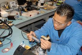
IPC J-STD-001 Training For Certified IPC Specialist (CIS) - BEST Inc.
Hand on Demonstration 

Talk through the full demonstration, step-by-step just as you will be presenting to your students. By, “talk through” I mean out loud. Pretend that the students are in the room with you. Tell the students each thing you are doing. Don’t assume that the students are all familiar with everything you are doing. For example, Introduce the students to the soldering system. 

“This is the power source for the soldering system. It is powered on using this switch. This is how you change the soldering tip for this model of the soldering system.” 

The smallest details are important to the students and to develop good habits as a worker. 

Be specific about what you are doing and why. 

Another example, “After picking up the soldering iron, it is necessary to wipe the tip on a clean, damp sponge. This action is called, ‘Thermally shocking’ the iron tip. Thermally shocking the tip clean away oxides and the old solder that is on the tip.” 

You know what you are doing. The demonstration is explaining each step to the student so each student in the class knows what to do and why to do the action. You may feel strange sitting in an empty room talking to the chairs, but the preparation makes sure that you have fewer surprises on the day of the demonstration.

3 – Verify the Equipment for the Class.

Few things are more frustrating to a student than working with poorly functioning or non-functioning equipment. Sit at each work location that a student will use and verify that all of the tips are heating properly and that all of the necessary tips are available. Heat, clean, inspect, tin, and store each tip. Replace any tips that are highly oxidized, are damaged or do not heat properly.

Verify that all the hand tools necessary are available. 

Think through the process that the students will be attempting. Will the student need pliers? What about tweezers? Is there a tool available for lead forming the through-hole components? How about wire strippers?

Verification of the tools will reduce the amount of class time used by hunting down and replacing non-functioning equipment.

4 -Set up the Learning Environment.

Arrive in the classroom early or even a day ahead to make sure that the room is ready. Remember the details. Verify that all students will have an unobstructed view of the instructor and the presentation slides. Ensure that the room temperature is comfortable, but not too warm. The material in the training class isn’t exciting and it can be difficult for students to concentrate if the students are fighting sleep. A distraction-free, comfortable learning environment is crucial to learning.  

Make sure you have all the necessary pens to make drawings and other illustrations. Locate and have at hand any examples or other visual aids you will use. 

Verify that each student has access to a copy of the J-STD-001 document, a pad, and pen for taking notes and if the students will be allowed to keep the copy of the document, a highlighter to use on the document.

When the students arrive, they should see a set classroom with everything necessary to facilitate learning.

5 – Set up Class in the IPC Portal

Online exams are a reality. The IPC online portal has been updated and if a far cry from the nightmare of the 2015 version. That doesn’t mean it’s perfect.

Setting up as much of the class as possible well before the day of class will ensure that any issues met can be handled by the IPC support team before class.

Try to have the student’s names and functioning email address so that you can enter them into the class beforehand. Once the students are in the class, contact the students and verify that each person has received the enrollment email and that each student can access the testing site. Email changes, name changes or corrections, or any other records items that must be done by IPC take time. Your class is the most important thing on your agenda. However, IPC’s support team handles several hundred help calls each day. It takes time for the team to receive, process, update, and return a reply to your help requests. It’s not reasonable to assume that IPC will drop everyone else and focus solely on your issue.

Before your first IPC J-STD-001 class presentation, remember to review the materials, practice the demonstrations, verify the equipment, set up the learning environment, and set up the class in the IPC portal.

Most of the 5 things listed in this paper will become second nature as you continue to teach. Preparation is the key to any class. Even more so when the class is the first time you will make the presentation.

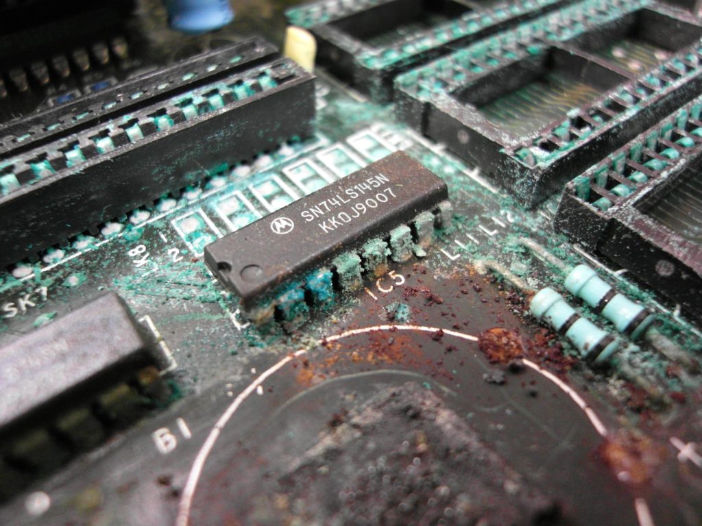
The Most Common PCB Repairs

Many terms tend to mixed together when people are discussing PCB repair. The resource for terms in electronics assembly can be found in the IPC T-50 which lists the terms and  definitions for electronic assemblies. Touch up, rework and repair often get intermingled. “Touch up” is done in the assembly process when alleged defects are identified and a heat source is brought onto the product in order to eliminate the defect. “Rework” refers to the action of re-processing a non-compliant product through the use of original or equivalent processing in a way which insures that the original applicable drawings or specifications are in compliance. For example, if post conformal coating the PCB has an area which should have had conformal coating but doesn’t, coating material can be applied to that area as a rework operation. The final coated board is required to be in compliance with the original coating specification. The “repair” of a product is an action in which a nonconforming product is restored to the functional capability. However, in the case of repair it does not assure compliance of the article with the original drawings or specifications.

Image result for most common pcb problems

As this definition of repair indicates the final product will not look like the original unit as signs of some of the repair work done will be visible. An example of this would be a burned hole in a board which has been fixed by removing the burned area and refilling it with epoxy. This will be visible and this is considered a repair process and it has to be be approved by the customer.

Listed below are the most common PCB repairs:

PCB land lifting/replacement

A PCB land is considered “lifted” off the board and is a defect per the IPC-A-610 inspection standards when it is pulled away from the PCB at least one thickness of the land. For a 1 ounce copper land the thickness is specified to be 1.4 mils (35 um) and therefore any “peeling” up of the land beyond this thickness would be considered a defect and can be repaired. This defect can occur when force, usually under temperature, is applied to the pad during device removal. In other cases there may be board handling damage which causes the pad to be lifted.

Image result for PCB land lifting/replacement

The repair of a lifted land can be accomplished via a variety of methods, but the IPC 7711/21 Rework, Modification and Repair of Electronic Assemblies defines two specific processes in the repair standard. One involves the use of epoxy to re-bond the lifted pad. Liquid epoxy is inserted under and around the lifted pad in order to re-attach it to the PCB. In the second method an epoxy film is used to bond the two materials back together. After placement of the dry film epoxy between the board and the pad, heat and pressure is applied to activate the adhesive an facilitate the repair.

The other variation on this type of SMT repair is that a conductor or trace is lifted or has been completely removed from the PCB.

PCB laminate damage

One of the next most common SMT repairs which occurs is damage to the laminate. Laminate damage occurs when there is improper board handling by personnel or when the protective packaging is not adequately applied to protect the PCB. There are a variety of methods which can be used to make this repair including an epoxy and a transplant method. In the epoxy method a temporary mold is created and epoxy is filled into the mold. After curing the epoxy is sanded to size and fit. In the replacement method a board of similar thickness and characteristics is “fitted” into the broken area.

Image result for PCB laminate damage

This is normally done when the damage is extensive and PCB assembly has enough value to warrant the repair time.

Mask damage

Another common physical damage to the PCB requiring repair is solder mask damage. This generally occurs when there is improper board handling, improper packaging and protection or during the PCB rework process. Solder mask can be repaired when replacement solder mask is dipped, brushed or sprayed onto the PCB subject to proper area definition via masking.

Image result for PCB solder Mask damage

While there are many other PCB repairs, those listed above are the most commonly observed. PCB repair can be accomplished on almost any PCB assembly, the only question is how much repair labor will be involved.

Hand Soldering Fundamentals and Rework Techniques

Hand soldering is the process of manually joining two metals through the use of soldering alloy, a heat source along with flux. This metal joining process has been around for several thousand years and has been adapted for modern electronic components with the tool of choice is a soldering iron. This writing explains several hand soldering fundamentals along with some aspects of PCB rework techniques.

The solders in most common use for the hand soldering of electronics are divided into “lead-free” and “tin-lead” alloy types. Their liquidus temperatures range from the mid 150 °C to 300 °C range.

Hand Soldering of Electronics

Reliable solder connections can only be accomplished with cleaned surfaces with the cleaning agent being a flux. Flux materials are made from a variety of materials and are either not cleaned up post soldering (“no-clean” fluxes) or are cleaned with water (“water-soluble” fluxes) or in some cases with other cleaning agents. The fluxes are formulated such that they provide consistent cleaning action during the soldering process while also serving as a wetting agent in order to get the solder to “flow” during the reflow process. Both of these actions lead to strong intermetallic bonds between the component lead and PCB surface to form a firm mechanical bond. These fluxes need to be “activated” at the right temperature and if proper hand soldering techniques are used little to no unspent flux residue is left on the PCB surface post hand soldering.

Soldering irons come in a variety of sizes and shapes to provide the heat necessary in order to get the solder to flow in a liquidus state. The soldering iron tip should be cleaned by wiping it on a wet sponge prior to soldering. The soldering iron is there to control the rate at which the work gets hot, how hot the tip gets, as well as how long it stays hot in order for a reliable solder joint to be formed. The soldering iron tip forms the heat bridge between the two surfaces which are soldered together. Its size should be matched to the pad/lead surface area as well as thermal mass (i.e. the thermal energy required to maintain a soldering temperature). The tip is in contact with both the pad and component with a tinned (i.e. solder on the tip) tip improving the thermal bridge. Solder on the tip of the soldering iron will make sure that there is a rapid transfer of heat into the component-PCB interface.

PCB Repair Materials and Tools

Before applying solder, the surface temperature of the parts being soldered must be raised to a point above the liquidus temperature of the solder.

Solder applied to a surface which has been cleaned, fluxed and heated to the right temperature based on the solder alloy will melt and flow. It should provide a smooth, even surface, feathering out to the edges of the structures being soldered. For an appropriate solder joint to be formed, the parts being soldered together should be held in place until the solder solidifies.

Depending on the flux being used, cleaning the solder joint area may be required. Cleaning of the solder joint area requiring cleaning will ensure the reliability of the solder interconnection. Post cleaning the PCBs should be dried using a nonparticulate-generating cloth or air source.

One of the common soldering joint anomalies is a disturbed solder joint. A disturbed joint has a rough, irregular appearance and looks dull instead of bright and shiny. It is the result of there be movement of the elements being soldered together during the time the solder is on the liquidus state. A disturbed solder joint may be unreliable and may require “touching up” or rework. A disturbed solder joint will usually require only reheating and reflowing of the solder with the addition of the same flux type used during the original assembly process. If this “touch up” does not correct the condition, the solder should be removed and the joints re-soldered.

It always best to not touch up any solder joints. However, when re-soldering is required, quality standards for the re-soldered connection should be the same as for the original connection. IPC standards for inspection criteria for such solder joints based on the class of the assembly are well documented.

If parts need to swap out for new this is considered PCB rework. The standard methods for reworking different component styles are outlined in IPC 7711 “Rework of Electronic Assemblies”.